 |
7-1: Technologies |
|
|
7-1: Technologies |
|
A technology is an environment in which design is done. Technologies can be layout specific, for example MOSIS CMOS, or they can be abstract, for example Schematics and Artwork. There are multiple CMOS variations to handle popular design rules such as MOSIS, D.O.D., and even round geometry. A simple Bipolar technology is available. Even Gallium Arsenide technologies have been built into Electric, but because they made use of proprietary design-rules, they are not distributed with the system.
The library "samples.txt" contains a number of examples of the different technologies in Electric (you can read it with the Readable Dump subcommand of the Import command of the File menu). The table below lists the examples:
| Cell | Technology | Description |
| tech-MOSISCMOS | mocmos | MOSIS CMOS rules |
| tech-RoundCMOS | rcmos | Experimental round CMOS rules |
| tech-nMOS | nmos | n-Channel MOS rules |
| tech-SchematicsDigital | schematics, digital | Digital schematics layout |
| tech-SchematicsAnalog | schematics, analog | Analog schematics layout |
| tech-PCB | pcb | Printed-circuit board layout |
| tech-DigitalFilter | efido | Digital filter architecture |
| tech-GEM | gem | Temporal logic specification |
| tech-Artwork | artwork | Graphical design |
Electric makes no restrictions about mixing components from different technologies. While editing a cell, you can switch technologies and start using new components along side the ones from the former technology. It is up to the designer to ensure that the resulting circuit is sensible.
Each technology consists of a set of primitive nodes and arcs. These, in turn, are constructed from one or more layers. Each technology also includes information necessary to do design, such as design rules, connectivity rules, simulation attributes, etc.
Within a technology, there are three classes of primitive nodes: pins, components, and pure-layer nodes. The pins are used to join arcs, so there is one pin for every arc in the technology. The components are the basic nodes used in design: contacts, transistors, etc. Finally, the pure-layer nodes are used for geometric manipulation, so there is one for every layer in the technology.
The component menu on the left side of the editing window contains arcs at the bottom (the menu entries with red borders), pin nodes above that (these appear as boxes with a cross inside), and components at the top (the more complex layer combinations). The pure-layer nodes are not in the components menu, but are available from the New Pure-Layer Node command of the Edit menu (see Section 6-10). Note that if you use the Components Menu... command of the Windows menu, and increase the number of menu entries, then the pure-layer nodes will be visible in the components menu.
When Electric begins, the status area shows the current "Technology". To work with a different technology, use the Change Current Technology... command of the Technology menu. This will prompt you with a list of available technologies. Once a choice is made, the component menu on the left will be redrawn to show the primitive nodes and arcs in the new technology. Because each technology has its own transparent colors, you will also notice a chromatic change in the display.
Electric automatically switches the current technology to match the cell being edited. If there are multiple cells being edited from different technologies, this switching can become annoying. To disable automatic technology switching, use the Cell Options... command of the Cells menu and uncheck "Switch technology to match current cell".
To see a list of primitive nodes and arcs in the current technology, use the Describe Current Technology command of the Technology menu. To get a detailed list of layer, node, and arc information in a technology, use the Document Technology command.
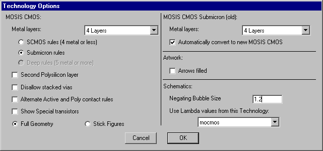
Some technologies have settable options that further customize them. The Technology Options... command of the Technology menu provides a dialog for controlling those options. More information about this dialog is available from the individual technology sections on MOSIS CMOS (Section 7-5), Schematics (Section 7-6), and Artwork (Section 7-7).
 |
Previous |  |
Table of Contents | Next |  |