 |
7-4: The MOS Technologies |
|
|
7-4: The MOS Technologies |
|
There is one nMOS technology: "nmos" (the specifications used in the Mead and Conway textbook).
There are many more CMOS technologies available. The most basic is "cmos", which uses an idealized set of design-rules from a paper by Griswold. The "mocmos" process has two layers of polysilicon and up to 6 layers of metal with standard, submicron, or deep rules (this is the default technology, and it is described more fully in the next section). There is even "rcmos", which uses round geometry!
 | Each MOS technology has two transistors (enhancement and depletion in nMOS technologies, n and p in CMOS). These nodes can have serpentine paths by highlighting them and using the Outline Edit command of the Edit menu (see Section 6-10). |
| The contact cuts in the MOS technologies automatically increase the number of cut layers when the contact grows in size. For very large contacts, however, the display of these cuts can waste time. Therefore, when very large contacts are displayed at small scale, the interior cuts are not drawn (as shown on the right). Be assured, however, that the cuts are actually there, and will appear in all appropriate output. | 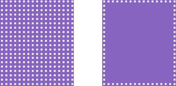 |
Although individual MOS nodes and arcs have the proper amount of implant around them, a collection of such objects may result in an irregular implant boundary. To clean this up, you can place pure-layer nodes of implant that neatly cover the implant area. Also, you can do this automatically with the Coverage Implants subcommand of the New Special Object command of the Edit menu.
 |
Previous |  |
Table of Contents | Next |  |