
9-2-3: Design Rules
Chapter 9: Tools
|
9-2: Design Rule Checking (DRC) 9-2-3: Design Rules |
|
Four types of errors are detected by the incremental and hierarchical design-rule checkers. Spacing errors are caused by geometry that is too close, but not connected. Notch errors are caused by geometry that is too close, but connected. Minimum size errors are caused by geometry that is too small. Resolution errors are caused by geometries that are smaller than a specified limit.
In addition to examining geometry, the design-rule checkers use connectivity information to help find violations. This use of network information helps the designer to debug circuit connectivity. For example, if two overlapping nodes are not joined by an arc, they may be considered to be in violation, even if their geometry looks right. This is because the checkers know what is connected and have a separate set of rules for such situations.
To help guide the design-rule checker, an "exclusion" layer can be placed over areas that are not to be examined. This exclusion layer is created by clicking the "Misc." entry of the component menu and selecting "DRC Exclusion" (see Section 7-6-3). Any errors that fall inside of this node's area are ignored.
To edit the design rules, use the Design Rules Preferences (in menu File / Preferences..., "Technology" section, ""Design Rules" tab). The dialog allows you to examine and modify the spacing limits for the current technology. Each rule has a numeric value (size or distance) as well as a textual description of the rule. The dialog is divided into two parts: "Node Rules" and "Layer Rules".
In the "Node Rules" section, you may set the minimum size of each node in the current technology.
In the "Layer Rules" section, you may set the minimum size, area, and enclosure area of each layer. You may also set the inter-layer spacing (between the "From Layer" and the "To Layer"). Use the "Show only 'to' entries with rules" to restrict the displayed rules to those with valid values.
The layer-to-layer spacing rules appear in 3 forms: normal, wide, and multicut. Normal rules come in three flavors: connected, unconnected, and edge. The connected rules apply to pieces of geometry that are electrically connected; the unconnected rules apply to unconnected geometry; edge rules apply to unconnected layers and ignore overlap when considering spacing distance.
The wide rules apply to large geometry. Although some technologies may have many different rules for different definitions of "large", the MOSIS CMOS technology has only one such rule. Additional rules can be controlled with the "Add Wide Rule" and "Delete Wide Rule" buttons.
The bottom of the dialog has a "Min resolution" field, which is the minimum resolution that can be manufactured.
|
If zero, no resolution check is done. When checking resolution, all geometry of that size or less will be flagged as resolution errors. For example, current MOSIS rules require that no boundaries be quarter-unit or less, so a value of .25 in this field will detect such violations. When rules have been changed, they are saved with your Preferences. To save them independently of the Preferences, use the Export DRC Deck... command (in menu Tools / DRC) to write an XML file with the design rules. Use the Import DRC Deck... command to restore these rules. | 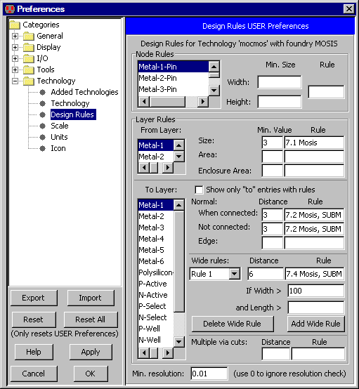 |
Note that the MOSIS CMOS design rule 6.7b is not checked by Electric because it is difficult to detect properly. This error is never fatal, and the worst case of missing this error is that active and poly are closer by 1/2 grid unit, which merely results in an increase in capacitive coupling between them. If this fringing capacitance is important, you've probably got so much polysilicon in your circuit that it has bigger problems.
 |
Previous |  |
Table of Contents | Next |  |