1-12-3: Layout
Chapter 1: Introduction
| 1-12: Schematics and Layout Tutorial 1-12-3: Layout |
Now that you have a schematic, it is time to draw the layout. Use the New Cell command (in menu Cell) to bring up the new cell dialog. Enter "nand2" as the cell name and "layout" as the view. Notice that the Components change from schematic symbols to layout primitives. The default technology is "mocmos" (MOSIS CMOS) but can be changed with the pop-up menu at the top of the Components tab. The "mocmos" technology has many options, such as the number of metal layers. To see these options, use the Preferences command (in menu File), and choose the "Technology" tab. In the "MOSIS CMOS" section, set the number of Metal layers to 6. (This preference is remembered, and you will not have to set it again in future sessions with Electric.) See Section 7-4-2 for more on the MOSIS CMOS technology.
 |
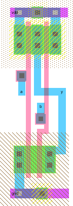
Your goal is to draw a layout like the one shown here. It is important to choose a consistent layout style so that various cells can "snap together." In this project's style, power and ground run horizontally in Metal-2 at the top and bottom of the cell, respectively. The spacing between power and ground is 80 units, center to center. No other Metal-2 is used in the cell, allowing the designer to connect cells with Metal-2 over the top later on. nMOS transistors occupy the bottom half of the cell and pMOS transistors occupy the top half. Each cell has at least one well and substrate contact. Inputs and outputs are given Metal-1 exports within the cell. You may find it convenient to have another sample of layout visible on the screen while you draw your gate. Use the Place Cell Instance command (in menu Cell) and select "inv{lay}". Then click to drop this inverter in the layout window. To view the contents of the inverter, highlight the inverter and use the One Level Down command (in menu Cell / Expand Cell Instances), or click on the "opened eye" icon in the toolbar. |
The inverter instance is really just a node, and its contents are unavailable for editing. To extract the contents, so that the individual nodes and arcs are available for editing, use the Extract Cell Instance command (in menu Cell). Note that this command flattens makes a copy of the inverter cell inside of your NAND cell. Study the inverter until you understand what each piece represents.
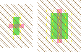
| Start by drawing your nMOS transistors. Recall that an nMOS transistor is formed when polysilicon crosses N-diffusion. N-diffusion is represented in Electric as green diffusion, surrounded by a dotted yellow N-select layer all within a hashed brown P-well background. This set of layers is conveniently provided as a 3-terminal transistor node in Electric. Move the mouse to the Components tab on the left side of the screen. |  |
As you move the mouse over various nodes, their name will appear in the status area at the bottom of the screen. Click on the N-Transistor, and click again in the layout window to drop the transistor in place. To rotate the transistor so that the red polysilicon gate is oriented vertically, use the 90 Degrees Counterclockwise command (in menu Edit / Rotate), or just type Ctrl-J. There are two nMOS transistors in series in a 2-input NAND gate, so we would like to make each wider to compensate. Double-click on the transistor (or type Ctrl-I). In the node properties dialog, adjust the width to 12.
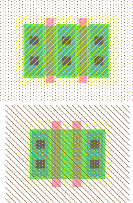
We need two transistors in series, so copy and paste the transistor you have drawn. You can also duplicate the selected object with the Duplicate command (in menu Edit) or just type Ctrl-M. Drag the two transistors along side each other so they are not quite touching. Click the diffusion (source/drain) of one of the transistors and right click on the diffusion of the other transistor to connect the two. Notice that Electric uses nodes and arcs in IC layout as well as in schematics. Once connected, drag the two transistors until the polysilicon gates are 3 units apart, looking like they do below. You will probably find it helpful to turn on the grid (type Ctrl-G). The grid defaults to small dots every unit and large dots every 10 units. You can change this with the Preferences command (in menu File), "Display" section, "Grid" panel. Change the "Frequency of bold dots" to 7, because the cells in this library have a wire pitch of seven.
You can move objects around with the arrow keys on the keyboard. The distance that they move defaults to 1 unit, but this can be changed by using the "Make grid larger" or "Make grid smaller" icons in the toolbar (or by pressing the "f" or "h" keys). You will avoid messy problems by keeping your layout on a unit grid as much as possible. Inevitably, though, you will create structures that are an odd number of units in width and thus will have either centers or edges on a half-unit boundary. (To move an object 7 units per click, or the equivalent of one bold-spaced unit, press Control and then press the appropriate arrow key. If you first hit "h" and then the control-arrow key will move an item one-half the distance of a bold-spaced unit, 3.5 in this case.)
Electric has an interactive design rule checker (DRC). If you place elements too closely together, it will report errors in the "Messages" window. Try dragging one of the transistors until its gate is only 2 units from the other. Observe the DRC error. Then drag the transistors back to proper spacing. When you are in doubt about spacing, you can recheck the cell with the Check Hierarchically command (in menu Tools / DRC), or just type the F5 key.
|
Next we will create the contacts from the N-diffusion to Metal-1.
Diffusion is also referred to as "active".
Drop a Metal-1-N-Active-Contact node in the layout window and double-click to change its Y size to 12.
You will need a second contact for the other end of the series stack of nMOS transistors, so duplicate the contact you have drawn (type Ctrl-M).
Move the contacts near each end of the transistor stack and draw diffusion lines to connect to the transistors.
A quick way to connect many items that are touching is to use the "auto router". To do this, select all of the objects to be routed (click and drag a selection box over them) and use the Auto-Stitch Highlighted Now command (in menu Tools / Routing), or just type the F2 key. See Section 9-6-2 for more on auto-stitching. |  |
Once the contacts are connected to the transistors you will need a gap of only 1 unit between the metal and polysilicon. Use the design rule checker to ensure you are as close as possible but no closer. Using similar steps, draw two pMOS transistors in parallel and create contacts from the P-diffusion to Metal-1. At this point, your layout should look something like this.
Draw wires to connect the polysilicon gates, forming inputs "a" and "b", and the Metal-1 output node "y". Then add Metal-2 power and ground lines. You can create these Metal-2 wires by creating a "Metal-2-Pin" node and right-clicking on it to draw a wire. Use the grid to make sure that the Metal-2 wires are 80 units apart. This is the same spacing as the power/ground lines of the inverter. Note that when two objects are selected, the Properties dialog box (Ctrl-I), also tells the distance between them.
A via, called "Metal-1-Metal-2-Con", is required to connect the Metal-1 to the Metal-2 lines. Select an active contact and right-click to connect it to the ground line. Electric will automatically create the necessary via for you while making the connection. Complete the other connections to power and ground. Let power and ground extend 2 units beyond the contents of the cell (excluding wells) on either side so that cells may "snap together" with their contents separated by 4 units (so design rules are satisfied).
Recall that well contacts are required to keep the diodes between the cells and source/drain diffusion reverse biased. We will place an N-well contact and a P-well contact in each cell. It is often easiest to drop the "Metal-1-N-Well-Con" near the desired destination (near VDD), then right click on the power line to create the via. Then drag the contact until it overlaps the via to form a stack of N+ diffusion, the diffusion to Metal-1 contact, Metal-1, the Metal-1-Metal-2-Con, and Metal-2. Repeat with the P-well.
In our datapath design style, we will be connecting gates, with horizontal and Metal-2 lines. Metal-2 cannot connect directly to the polysilicon gates. Therefore, we will add contacts from the polysilicon gate inputs to Metal-1 to facilitate connections later in our design. Place a "Metal-1-Polysilicon-1-Con" node near the left polysilicon gate. Connect it to the polysilicon gate and drag it near the gate. You will find a 3 unit separation requirement from the Metal-1 in the contact to the metal forming the output "y". Add a short strip of Metal-1 near the contact to give yourself a landing pad for a via later in the design. You may find Electric wants to draw your strip from the contact in polysilicon rather than Metal-1. To tell Electric explicitly which layer you want, click over the Metal-1 arc in the Component tab (arcs have red borders). Then draw your wire.
Electric is agnostic about the polarity of well and substrate; it generates both n- and p-well layers. In our process that has a p-substrate already, the p-well, indicated by brown slanting lines, will be ignored. The n-well, indicated by small brown dots, will define the well on the chip. Electric only generates enough well to surround the n and p diffusion regions of the chip. (Electric creates well contacts that are only 11 units wide! This will generate a DRC error, but this behavior is intentional. Wells should be 12 units wide to meet DRC's expectations.) It is a good idea to create rectangles of well to entirely cover each cell so that when you abut multiple cells you don't end up with awkward gaps between wells that cause design rule errors. To do this, click on the "Pure" entry of the Components tab and select "N-Well-Node" or "P-Well-Node". To change its size so that it entirely covers the existing well, resize it with the Interactively command (in menu Edit / Size) or just type Ctrl-B. You will find the pure layer nodes are annoying because you will tend to select them when you really want to select a transistor or wire. To avoid this problem, select them and use the Make Selected Hard command (in menu Edit / Selection) to make the node hard-to-select. Once an item is defined as hard-to-select, you must use "special select" mode to be able to select it (click on the arrow with the letters "SP" in the toolbar). You can use the Make Selected Easy command if you want to restore a node or arc to be easily selected. Electric also provides the Coverage Implants Generator command (in menu Tools / Generation) that automatically creates hard-to-select pure layer nodes for N and P wells. This command is convenient for simple geometries inside of a cell.
Create exports for the cell. When you use the cell in another design, the exports define the locations that you can connect to the cell. Click near the end of the short Metal-1 input line that you just drew on the left gate, and select the Metal-1-Pin node. If you accidentally select the Metal-1 arc instead, click elsewhere in space to deselect the arc, then try again to find the pin. You may also try holding the Control key while clicking to cycle through everything that is under the cursor. Add an input export called "a" (type Ctrl-E to get the export dialog). Repeat for input "b". Export output "y" from the metal line connecting the nMOS and pMOS transistors. You may have to place an extra pin and connect it to the output line to give yourself a pin to export as "y". Also export "vdd" and "gnd" from the Metal-2 arcs; these should be of type power and ground, respectively. Electric recognizes "vdd" and "gnd" as special names, so be sure to use them.
| Previous | Table of Contents | Next |