
7-4-2: The MOSIS CMOS Technology
Chapter 7: Technologies
|
7-4: The MOS Technologies 7-4-2: The MOSIS CMOS Technology |
|
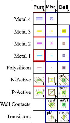 |
The MOSIS CMOS technology describes a scalable CMOS process that is fabricated by the MOSIS project of the University of Southern California. To obtain this technology, use the popup menu at the top of the component tab (in the side bar) and select "mocmos". This technology can have from 2 to 6 layers of metal (4 are shown here, 6 is the default). It has 1 polysilicon layer but can be changed to use 2. The technology can be set to use either standard rules (SCMOS), submicron rules, or deep rules. You can choose whether to allow stacked vias and whether or not to use alternate contact rules. Finally, you can set the technology into "Analog" mode, which provides an NPN transistor, a Polysilicon Capacitor, and many resistors. This is done with the Technology Preferences (in menu File / Preferences..., "Technology" tab). |
The default orientation of transistors (both in the menu, and when first placed) can be rotated by checking "Rotate transistors in menu" in the Technology Preferences.
Users of Electric version 6.02 or earlier will have a different MOSIS CMOS technology called "mocmossub". This technology attempted to match the submicron rule set, but did not do so as accurately as the current "mocmos" technology. If you have designs in that technology, they will be automatically converted to the new "mocmos" when read in.
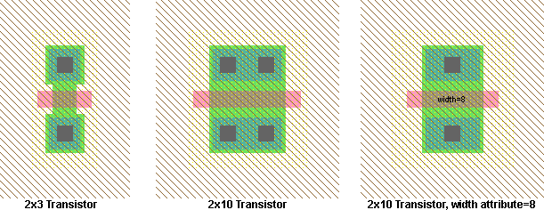
The MOSIS CMOS technology has two transistor nodes that can take a text attribute to control their width. These transistors also have contacts built into them. Without the text attribute, the maximum width is displayed. However, by adding a "width" attribute, they shrink to that size. Note that the ports never change location, thus allowing them to scale without triggering constraints. The scaling feature of these transistors is not very useful because it is not possible to parameterize layout cells.
|
The scalable transistor on the left is 3 wide, and the other two are 10 wide. However, the scalable transistor on the right has the "width" set to 8, so it has shrunk. If you get Object Properties... on a scalable transistor, there are extra controls that let you choose to have fewer contacts (1 or even none), and you can tighten the contact spacing. | 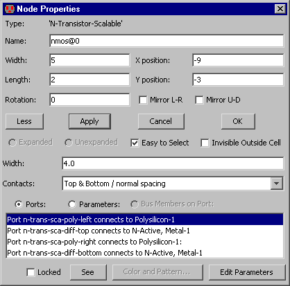 |
 |
Previous |  |
Table of Contents | Next |  |