7-3: I/O Specifications |
7-3: I/O Specifications |
Unfortunately, many of these formats are pure geometry with no information about the circuit connections. When read, the input formatter creates pure-layer nodes to describe the geometry. This means that transistors, contacts, and other multi-layer nodes are not constructed properly. Although the cell appears visually correct, and can be used to export the same type of file, it cannot be analyzed at a circuit level.
A partial solution to this problem exists now. The Node Extract subcommand of the Network command of the Tools menu will replace the pure-layer nodes in the current cell with connected nodes and arcs. It isn't guaranteed to work in all situations, and it doesn't recognize transistors at all. However, it starts the conversion process (which must be completed by hand). Also, the code is available and some enterprising programmer may want to finish (or rewrite) it.
CIF options are controlled with the CIF Options... subcommand of the IO Options command of the File menu.
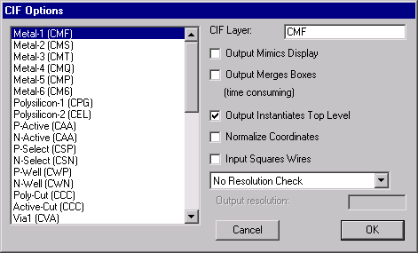
This dialog controls the conversion between layers in Electric and layers in the CIF file. By clicking on an Electric layer, you can type a new CIF layer into the dialog.
By default, CIF output writes the entire hierarchy below the current cell. If you check the "Output Mimics Display" item, cell instances that are unexpanded will be represented as an outline in the CIF file. This is useful when the CIF output is intended for hardcopy display, and only the screen contents is desired. To revert to the default state, uncheck the item.
Another option is whether or not to merge adjoining geometry. This is an issue because of the duplication and overlap that occurs wherever arcs and nodes meet. The default action is to write each node and arc individually. This makes the file larger because of redundant box information, however it is faster to generate and uses simpler constructs. If you check the "Output Merges Boxes" item, all connecting regions on the same layer are merged into one complex polygon. This requires more processing, produces a smaller file, and generates more complex constructs.
Another option is whether or not to instantiate the circuit in the CIF. By default, the currently displayed cell becomes the top level of the CIF file, and is instantiated at the end of the CIF. This causes the CIF file to display the current cell. If the CIF file is to be used as a library, with no current cell, then uncheck the "Output Instantiates Top Level" checkbox, and there will be no invocation of the current cell.
The "Normalize Coordinates" option causes the coordinate system of each CIF cell to be centered at zero.
When reading CIF files, the CIF "wire" statements are assumed to have rounded geometry at the ends and corners. If you check the "Input Squares Wires" item, CIF input assumes that wire ends are square and extend by half of their width.
You can request that resolution errors be checked during CIF output. In addition, by selecting "Show Resolution Errors", the errors are can be reviewed, one at a time, after CIF output is done. The "Output resolution" field is the minimum coordinate value that can be safely written in CIF (due to CIF's use of the centimicron as the smallest unit). All geometry of that size or less will be flagged during CIF output. For example, current MOSIS rules require that no boundaries be quarter-lambda or less, so a value of .25 in this field will detect such violations.
GDS options are controlled with the GDS Options... subcommand of the IO Options command of the File menu.
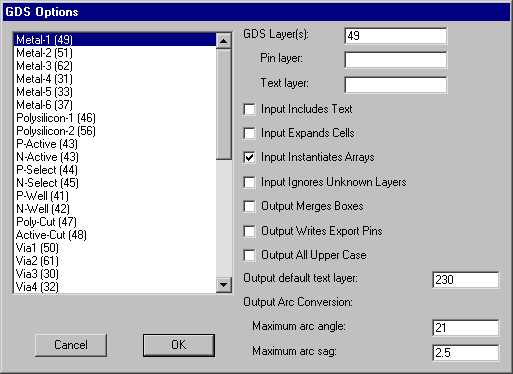
In GDS files, there are no names for each layer, just numbers. It is important that Electric know the meaning of each number so that it can properly read and write GDS files. This dialog lets you edit those GDS layer numbers and assign them to different Electric layers.
The list on the left shows all of the Electric layers. By clicking on a layer name, its GDS layer numbers are shown in the top-right and can be edited. You can place multiple GDS layer numbers in the field, separated by commas. When you do this, all of those numbers will be accepted when reading GDS (but only the first will be used when writing GDS). In addition to GDS layer numbers to use for layout, there are also two other types of GDS layer numbers: a pin layer (for exports) and a text layer (for export names).
These dialog elements apply to reading GDS:
These dialog elements apply to writing GDS:
EDIF options are controlled with the EDIF Options... subcommand of the IO Options command of the File menu.
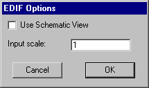
This dialog controls whether EDIF output writes schematic or netlist views (the default is netlist). It also lets you set a scale factor for EDIF input.
DEF options are controlled with the DEF Options... subcommand of the IO Options command of the File menu.
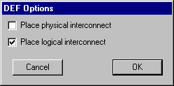
This dialog controls whether DEF reads physical and/or logical information.
CDL options are controlled with the CDL Options... subcommand of the IO Options command of the File menu.
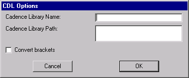
This dialog control the library name and path information that is written, and it lets you control the conversion of square-bracket characters.
DXF options are controlled with the DXF Options... subcommand of the IO Options command of the File menu.
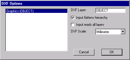
This dialog controls the conversion between layers in Electric and layers in the DXF file. By clicking on an Electric layer, you can type a new DXF layer into the dialog.
By default, Electric flattens DXF input, removing levels of hierarchy and creating a single cell with the DXF artwork. By unchecking the "Input flattens hierarchy", Electric will preserve the structure of the DXF file.
If a layer name in the DXF file is not found in the list that you setup in Electric, it will be ignored. If you check "Input reads all layers", then all layers are read into Electric, regardless of whether the layer names are known.
To control scaling, you can change the meaning of units in the DXF file. The default unit is "Millimeters", which means that a value of 5 in the DXF file becomes 5 millimeters in Electric.
SUE input is controlled with the SUE Options... subcommand of the IO Options command of the File menu.

This dialog controls whether transistors will appears in a standard 3-terminal configuration or in a 4-port configuration with a substrate connection.
| Previous | Table of Contents | Next |