9-9: Silicon Compiler |
9-9: Silicon Compiler |
Be warned that the silicon compiler is rather old, and so it produces layout that alternates standard cell rows and routing rows. Modern silicon compilers use 3 and 4 metal processes to route over the standard cells, but this system does not.
The VHDL description is normally placed in the "vhdl" view of a cell. It can be created and edited entirely inside of Electric, or it can be read from disk by using the Read Text Cell... command of the Cells menu. See Section 4-10 for more on text editing. Automatic generation of VHDL from layout is done with the Make VHDL View command of the View menu.
Once the VHDL is created, it is compiled into a netlist and read into the silicon compiler. The netlist is normally placed in the "netlist-quisc-format" view of a cell. If the netlist is too cumbersome to retain in memory, it may be kept on disk by using the VHDL Options... subcommand of the VHDL Compiler command of the Tools menu and unchecking the "Netlist stored in cell" item. The "VHDL stored in cell" check controls the placement of VHDL text in a similar way.
When generating a schematic or VHDL description, it is important to know what primitives are available in the standard cell library. Electric comes with a CMOS cell library in the MOSIS CMOS ("mocmos") technology. This library is not correct, and exists only to illustrate the Silicon Compiler. These component declarations are available:
component and2 port(a1, a2 : in bit; y : out bit); end component;
component and3 port(a1, a2, a3 : in bit; y : out bit); end component;
component and4 port(a1, a2, a3, a4 : in bit; y : out bit); end component;
component inverter port(a : in bit; y : out bit); end component;
component nand2 port(a1, a2 : in bit; y : out bit); end component;
component nand3 port(a1, a2, a3 : in bit; y : out bit); end component;
component nand4 port(a1, a2, a3, a4 : in bit; y : out bit); end component;
component nor2 port(a1, a2 : in bit; y : out bit); end component;
component nor3 port(a1, a2, a3 : in bit; y : out bit); end component;
component nor4 port(a1, a2, a3, a4 : in bit; y : out bit); end component;
component or2 port(a1, a2 : in bit; y : out bit); end component;
component or3 port(a1, a2, a3 : in bit; y : out bit); end component;
component or4 port(a1, a2, a3, a4 : in bit; y : out bit); end component;
component rdff port(d, ck, cb, reset : in bit; q, qb : out bit); end component;
component xor2 port(a1, a2 : in bit; y : out bit); end component;
To use the silicon compiler, simply run the subcommands in the Silicon Compiler command of the Tools menu. The commands are organized in the menu so that, when run sequentially downward, they perform the compilation process. The steps are as follows:
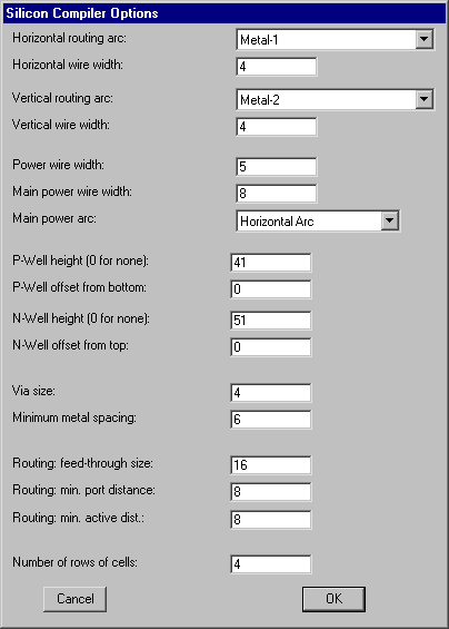
| Because cells are laid out in rows that run horizontally, the Vertical routing arc runs in and out of cells, while the Horizontal routing arc runs between the cells in the routing channel. The Power arcs run horizontally between the cells to connect both power and ground. The Main Power arcs run vertically along the sides of the circuit to connect the horizontal power and ground rails (you can choose which layer to use for the main power arcs). A block of P-well will be placed along the bottom of each cell and extend up to the P-Well height (if nonzero). A block of N-well will be placed along the top of each cell and extend down to the N-Well height (if nonzero). The offset of these blocks from the bottom or top can also be given. The Via size, Minimum metal spacing, Routing feed-through size, Minimum port distance, and Minimum active distance are rules that are used to place wires in the routing channel. |  |
The last subcommand in the Silicon Compiler command is Issue Special Instructions..., which does not normally need to be used. However, the silicon compiler system is so extensive that advanced users may wish to use it. After issuing this command, any sequence of silicon compiler instructions may be typed. Use the "Cancel" button to return to Electric.
| Previous | Table of Contents | Next |