 |
8-8: The Node Cells |
|
|
8-8: The Node Cells |
|
Nodes are the components in a technology, and they are constructed from pieces of geometry on the layers.
To edit an existing node, use the Edit Primitive Node... command of the Technology menu, and to create a new node use the New Primitive Node... subcommand of the New Primitive command. Once a node is being edited, the next one in sequence can be edited with the Edit Next Primitive command. The current node can be deleted with Delete this Primitive. Also, you can rename a node with the Edit Cell... command of the Cells menu, but remember to use the name "node-" in front (i.e. the old name is "node-metal1-metal2-contact" and the new name is "node-via"). Finally, you can rearrange the order in which the nodes will be listed by using the Reorder Primitive Nodes subcommand of the Reorder Primitives command.
The node cell contains four pictures of the node on the left and textual information on the right. You can update the textual information entries by highlighting them and using the technology edit button.
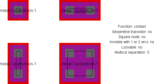
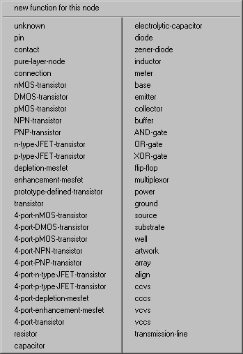
The "Function" entry describes the node's function, which is a different set than the arc and layer functions. The menu of possible node functions is shown here.
The "Serpentine transistor" entry indicates that this is a MOS transistor and it can take arbitrary outline information to describe its geometry.
 |
The "Square" entry forces the node to always have the same X and Y dimension when scaled.
The "Invisible with 1 or 2 arcs" entry indicates that the node will not be drawn if it is connected to exactly one or two arcs. This is useful in schematic pins, which are visible only when unconnected or forming a junction of 3 or more wires. The "Lockable" entry indicates that this node can be made unchangeable along with other lockable primitives, when the lock is turned on during editing (see Section 6-2 for more on locking these primitives). This is typically used in array technologies such as FPGA. The "Multicut separation" is the distance between multiple contact cuts when the node grows large. Although this distance can be automatically determined from the different examples, it can also be give explicitly here, and this allows you to draw only one example. |
For nodes, it is common to sketch four different examples of the node in varying scales, so that X and Y scaling rules can be derived (square nodes need only two examples). If only one example is specified, default scaling rules will be presumed.
The smallest example, called the main example, is used as the default size and also contains all of the special port information. Needless to say, it is important to keep the geometry of each example well apart from the others so that the technology editor can distinguish them.
Each example must contain the same geometric layers (only stretched). As in the Arc cells, pieces of geometry can be created by selecting from the component menu on the left, creating the geometry, and then using the technology edit button to assign a layer to the geometry. If any polygonal geometry is used (for example, the Filled polygon entry, sixth from the top), they require outline information to be assigned with the Outline Edit subcommand of the Special Function command of the Edit menu. If the Opened circle arc entry is selected (second from the bottom), you can specify the number of degrees of the circle with the Get Info command of the Info menu.
Each example must also contain a highlight layer to indicate the correct highlighting on the display. Select the "HIGH" entry in the menu on the left to create this special type of layer.
Each example must also contain port information. Select the "PORT" entry in the component menu to create this special type of layer. You will have to provide a name for each port, and the name must be the same on each example.
| Ports on the main example must also have connectivity information (which arcs can connect to them) and range information (the permissible angle of connected arcs). Use the technology edit button to set this (see the sample menu on the right). Each possible arc listed can have its connectivity set by typing "y" or "n" when pointing to its name in the menu. | 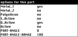 |
The range consists of two numbers: a main angle (in degrees counterclockwise from 3 O'clock) and a range about that angle. For example, a port angle of 90 with a port angle range of 45 describes a port that points upward and can connect at angles up to 45 degrees off from this direction. The range will be graphically depicted.
The ports on the main example must also indicate any internal electrical connectivity by actually connecting them together. For example, the two polysilicon ports on a MOS transistor should be connected in the main example. Use the selection and toggle select buttons on the two ports, then use the technology edit button to join the ports with a universal arc. Do not put this internal connection on any example other than the main one. To see the location of all ports on the main example, use the Identify Ports command.
Although the "grab point" is usually defined to be the center of the highlight area (unless the user unchecks "Center-based primitives" in the Selection Options dialog), this can be overridden by placing a Cell-Center node (named "Facet-Center" for historical reasons) at the appropriate location in the main example. Placing this mark on the left side will cause instances of the node to be placed by their left side rather than the center of the highlight area. To get this node, use the Cell Center subcommand of the New Special Object command of the Edit menu.
As with arcs, use the Identify Primitive Layers command to label each piece of geometry in the main example.
There are some special cases available in node descriptions. A piece of geometry in the main example may be changed (with the technology edit button) to SET-MINIMUM-SIZE. This indicates that the current size is the smallest possible, and it cannot scale any smaller (this is used by the "mocmos" technology for the metal layer in contacts). The restriction can be removed with the CLEAR-MINIMUM-SIZE description. This option cannot be used in serpentine transistors.
Another special case in node description is the ability to specify multiple cut layers. If the larger examples have more cut layers, rules are derived for cut size and spacing so that an arbitrary numbers of cuts can be inserted as the contact scales.
Although serpentine MOS transistors are a special case, they cannot be automatically identified, but must be explicitly indicated with a textual field on the right. Besides this explicit indication, the transistor node must contain four ports: two on the gate layer (polysilicon) and two on the gated layer (active). A standard geometry must be used that shows polysilicon and diffusion crossing in a central transistor area. Any deviation from this format may cause the technology editor to be unable to derive serpentine rules for the node.
Besides the standard nodes for transistors, contacts, and other circuit elements, it is necessary to build pin and pure-layer nodes. There should be one pin for every arc, so that the arc can connect to others of its type. The pin should be constructed of pseudo-layers (i.e. it has no real geometry), should have the "pin" function, and should have one port in the center that connects to one arc. The technology editor will issue a warning if there is no pin node associated with an arc.
The pure-layer nodes should also be built, one for each layer. They should have only one piece of geometry and have the "pure-layer" function. The technology editor will issue a warning if there is no pure-layer node associated with a layer.
 |
Previous |  |
Table of Contents | Next |  |