
Chapter 9: Tools
|
9-12: Silicon Compiler | |
Silicon compilation is the process of converting from a hardware description language (such as Verilog or VHDL) directly to placed and routed silicon. Electric has two ways of accomplishing this task. The old way uses a silicon compilation system called QUISC (the Queen's University Interactive Silicon Compiler).
The second way, which is more modern and powerful, uses Electric's separate tools for converting hardware description code, placing it, and routing it.
QUISC is a powerful tool that can do placement and routing of standard cells from a schematic or a structural VHDL description. The VHDL is compiled into a netlist which is then used to drive placement and routing. Schematics are first converted into VHDL, then compiled to a netlist and laid-out. Thus, a byproduct of silicon compilation will be a {net.quisc} view of a cell, and potentially a {vhdl} view.
Be warned that the silicon compiler is rather old, and so it produces layout that alternates standard cell rows and routing rows. Modern silicon compilers use multiple metal processes to route over the standard cells, but this system does not. This system uses two layers: a vertical routing arc to run in and out of cells, and a horizontal routing arc to run between the cells in the routing channel. It also uses power arcs to bring power and ground to the cell rows, and main power arcs to connect the rails on the left and right.
The VHDL description is normally placed in the "vhdl" view of a cell (see Section 4-9 for more on text editing). There is a VHDL example in cell "tool-SiliconCompiler{vhdl}" of the "samples" library. To access it, use the Load Sample Cells Library command (in menu Help).
To convert a schematic or VHDL cell into layout, use the Convert Current Cell to Layout command (in menu Tools / Silicon Compiler). To compile VHDL or Verilog to the {net.quisc} view, use the Compile VHDL to Netlist View or Compile Verilog to Netlist View commands. (these are typically not needed, since the previous command does it automatically).
When creating a schematic or VHDL cell to be compiled, it is important to know what primitives are available in the standard cell library. Electric comes with a CMOS cell library in the MOSIS CMOS ("mocmos") technology. This library is not correct, and exists only to illustrate the Silicon Compiler. These component declarations are available:
component and2 port(a1, a2 : in bit; y : out bit); end component;
component and3 port(a1, a2, a3 : in bit; y : out bit); end component;
component and4 port(a1, a2, a3, a4 : in bit; y : out bit); end component;
component inverter port(a : in bit; y : out bit); end component;
component nand2 port(a1, a2 : in bit; y : out bit); end component;
component nand3 port(a1, a2, a3 : in bit; y : out bit); end component;
component nand4 port(a1, a2, a3, a4 : in bit; y : out bit); end component;
component nor2 port(a1, a2 : in bit; y : out bit); end component;
component nor3 port(a1, a2, a3 : in bit; y : out bit); end component;
component nor4 port(a1, a2, a3, a4 : in bit; y : out bit); end component;
component or2 port(a1, a2 : in bit; y : out bit); end component;
component or3 port(a1, a2, a3 : in bit; y : out bit); end component;
component or4 port(a1, a2, a3, a4 : in bit; y : out bit); end component;
component rdff port(d, ck, cb, reset : in bit; q, qb : out bit); end component;
component xor2 port(a1, a2 : in bit; y : out bit); end component;
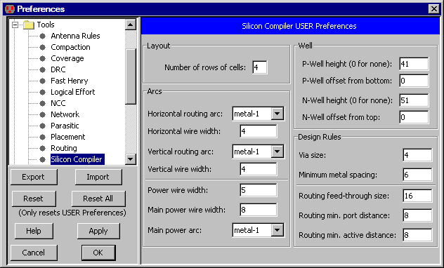
The Silicon Compiler Preferences (in menu File / Preferences..., "Tools" section, "Silicon Compiler" tab) let you control many aspects of placement and routing.
To do silicon compilation of Verilog or VHDL using the more advanced tools, a three step process is necessary:
After routing, you may want to redo the placement with different padding. You may also want to adjust the routing parameters to get better results, and you can always unroute and re-route individual networks.
 |
Previous |  |
Table of Contents | Next |  |