 |
1-10: IC Layout Example |
|
|
1-10: IC Layout Example |
|
| Before you can place any IC layout, the editing window must have a cell in it. Use the Edit Cell... command in the Cells menu. This will show a dialog with a list of existing cells (which is empty, because none exist yet). Click on the "New Cell" button at the bottom of this dialog to create a new cell. You will then see a dialog which asks you for information about this new cell. | 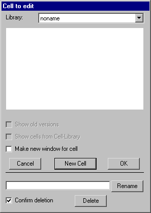 |
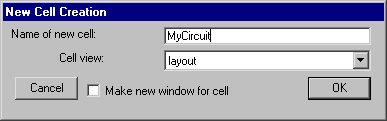 | Type the name ("MyCircuit" is used here) and click OK. The editing window will no longer have the "No cell in this window" message, and circuitry may now be created. |
| Layout is placed by selecting nodes from the components menu, and then wiring them together. This example shows two nodes that have been created. This was done by clicking on the appropriate component menu entry, and then clicking again in the editing window to place that node. After clicking on the component menu entry, the cursor changes to a pointing hand to indicate that you must select a location for the node. When placing the node, if you press the button and do not release it, you will see an outline of the new node, which you can drag to its proper location before releasing the button. | 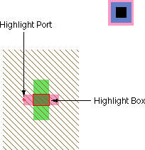 |
In this example, the top node is called Metal-1-Polysilicon-1-Con (a contact between metal layer 1 and polysilicon layer 1, found in the sixth entry from the bottom in the right column of the component menu). The node on the bottom is called N-Transistor (sixth entry from the top in the right column of the component menu). Both of these nodes are from the MOSIS CMOS technology (which is listed as "mocmos" in the status area).
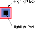 | A highlighted node has two selected areas: the node and a port on that node. Note that the transistor is highlighted in the example above, and the contact is highlighted in the example here. The larger selected area is the node, and it surrounds the "important" part of the node (for example, on the Transistor, it covers only the overlap area, excluding the tabs of active and gate on the four sides). The smaller selected area is the currently highlighted port (there are four possible ports on the transistor, but only one on the contact). |
To highlight a node, use the selection button. The node, and the closest port to the cursor, will be selected. After highlighting, you can hold the mouse button down and drag the highlighted object to a new location. If nothing is under the cursor when the selection button is pushed, you may drag the cursor while the button remains down to define an area in which all objects will be selected.
Another way to affect what is highlighted is to use the toggle select button. The toggle select button causes object highlighting to be reversed (highlighted objects become unhighlighted and unhighlighted objects are highlighted).
The shape of the highlighted port is important. Ports are the sites of arc connections, so the end point of the arc must fall inside this port area. Ports may be rectangles, lines, single points (displayed as a "+"), or any arbitrary shape. For example, when the active tabs of a transistor are highlighted, the port is shown as a line.
| To wire a component, select it, move the cursor away from the component, and use the creation button. A wire will be created that runs from the component to the location of the cursor. Note that the wire is a fixed-angle wire which means that it will be drawn along a horizontal or vertical path from the originating node. To see where the wire will end, click but do not release the button and drag the outline of the wire's terminating node (a pin) until it is in the proper location. It is highly recommended that you do all wiring operations this way, because wiring is quite complex and can follow many different paths. | 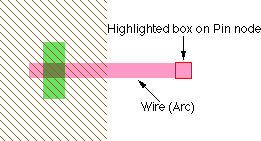 |
Once a wire has been created, the other end is highlighted (see above). This is the highlighting of a pin node that was created to hold the other end of the arc. Because it is a node, the creation button can be used again to continue the wire to a new location. If the creation command terminates over an existing component, the wire will attach to that component.
To remove wires or components, you can issue the Undo command of the Edit menu to remove the last created object. Alternatively, you can select the component and use the Erase command from the Edit menu.
Once components are wired, moving them will also move their connecting wires. Notice that the wires stretch and move to maintain the connections. What actually happens is that the programmable constraint system follows instructions stored on the wires, and reacts to component changes. The default wire is fixed-angle and slidable, so the letters "FS" are shown when the wire is highlighted.
Select a wire and issue the Rigid command of the Arc menu. The letters change to "R" on the arc and the wire no longer stretches when components move. Find another arc and issue the Not Fixed-angle command in the Arc menu. Now observe the effects of an unconstrained arc as its neighboring nodes move. These arc constraints can be reversed with the Rigid and Fixed-angle commands.
| Electric supports hierarchy by allowing you to place instances of another cell. These instances are nodes, just like the simpler ones in the component menu. To see hierarchy in action, create a new cell with the Edit Cell... command of the Cells menu. Click on the "New Cell" button at the bottom, and make sure the "Make new window for cell" option is checked in the dialog. Then type the new cell name ("Higher" is used in the example here) and set its view. | 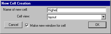 |
A new (empty) cell will appear in a separate window. Try creating a few simple nodes in this new window (place a contact or two).
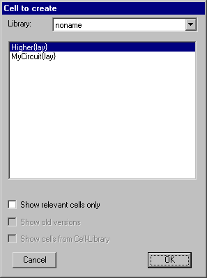 | Now place an instance of the other cell by using the New Cell Instance... command from the Edit menu. You will be given a list of cells to create: select the one that is in the OTHER window (the one called "MyCircuit" in this example). Then click in the newer cell to create the instance. |
| The box that appears is a node in the same sense as the contacts and transistors: it can be moved, wired, and so on. In addition, because the node contains subcomponents, you can see its contents by selecting it and using the One Level Down subcommand of the Expand Cell Instances command in the Cells menu. Note that if the objects in a cell no longer fit in the display window, use the Fill Window command from the Windows menu. |  |
Before you can attach wires to the instance node, there must be connection sites, or ports on that node. Primitive nodes such as contacts and transistors already have their ports established, but you must explicitly create ports for cell instances.
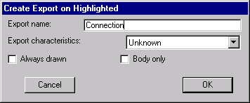 | This is done by creating exports inside the cell definition. Move the cursor to the window with the lower-level cell ("MyCircuit") and select the contact node. Then issue the Create Export... command from the Export menu. You will be prompted for an export name and its characteristics (the characteristics can be ignored for now). |
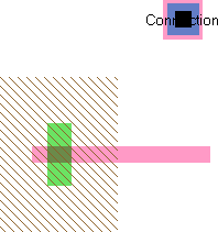 |
This takes the port on the contact node and exports it to the outside world.
Its name will be visible on the unexpanded instance node in the higher-level cell.
You can now connect wires to that node in just the same way as you wired the contact. | 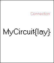 |
Some final commands that should be mentioned in this introductory example are the Save Library and the Quit commands which can be found in the File menu. They do the obvious things. Also, the Help... command from the Info menu is very useful. It displays a dialog with a list of subjects and offers information about each one.
 |
Previous |  |
Table of Contents | Next |  |