 |
|
|
|
In this first example, the user simply wishes to change the Metal-2 layer from a solid fill to a stipple pattern.
This particular task is so basic that it can be done with the Layers Preferences, but it illustrates the basic steps of making a change. First, edit the layer cell for "metal-2". The display will show the layer with all of its associated information.
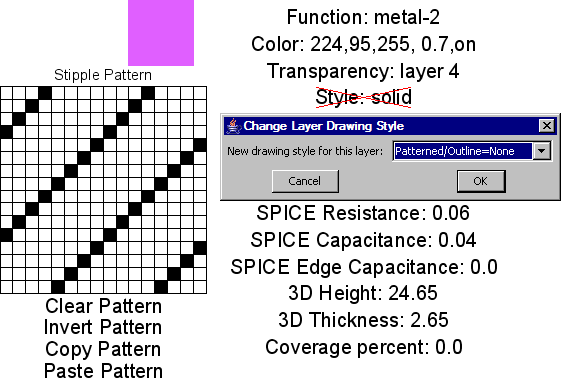
Because every layer has a default stipple pattern used for printing, all that is necessary is to change the "Style" field from solid to patterned. To do this, double-click on the "Style" text and select "Patterned/Outline=None". The technology is now modified and can be converted back with the Convert Library to Technology... command.
The second example is more extensive: creation of a new primitive node. In this case, the new node is a contact between metal-2 and polysilicon.
| To create the node, use the context menu on the "TECHNOLOGY NODES" tab of the explorer window, select "Create New Node", and name the node appropriately. | 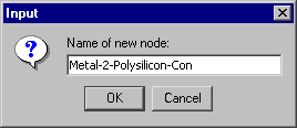 |
At this point, the display will show only the textual information about the node (because the graphical information is yet to be supplied). The textual information consists of five factors that now fill the screen.
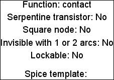 | You should begin by changing the "Function" factor to "contact" (double-click it and select the appropriate function). Then pan back so there is room to describe the node graphically. The other factors are properly set for a contact. |
| To place a piece of geometry (for example, some polysilicon), click over the Filled Box entry in the component menu (third from the top) and then click in the edit window. This geometry now has shape, but no layer associated with it. To assign a layer, double-click on the geometry. Then choose "polysilicon-1". The black box will change appearance to that of a polysilicon layer. You can move and stretch this box appropriately. | 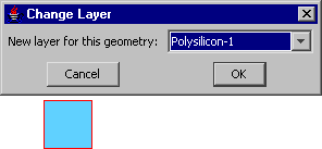 |
In this example, assume that a contact between polysilicon and metal-2 has three layers: polysilicon-1, metal-2, and contact cut. Therefore, the above operation must be done two more times to place the metal-2 and contact cut layers.
Besides this pure geometry, there must be two other items in the node: a highlight layer and a port. The highlight layer is obtained by selecting the "HIGH" entry from the component menu. It is then placed and stretched so that it encloses the contact (highlight layers define the size of the node, and this means that they will typically surround the geometry).
 |
The other item that must be created is a port
(more than one can be created, but for contacts, one is sufficient).
Select the "PORT" entry from the menu on the left and place it in the display.
You will be prompted for a port name, after which you can further move or stretch the port.
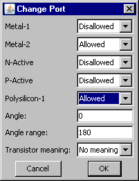
Besides a location and a name, ports must specify which arcs may connect to them.
To do this, double-click on the port.
The resulting menu lists all of the arcs and indicates possible connectivity. Note that the last two entries define the permissible range of angles to which arcs may connect. For a contact such as this, arcs may connect at any angle, so the default values are correct. |
| When all of the geometry, highlighting, and ports have been placed, you can double-check your work with the Identify Primitive Layers command (in menu Edit / Technology Editing), which will display this information (note that the port name "Center" has been moved away for clarity): | 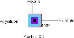 |
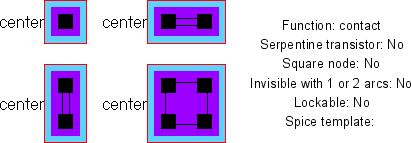
The final step in the definition of this node is to create three more copies that illustrate scaling in both axes. This is done simply by selecting all five objects and using the Duplicate command (in menu Edit). Once duplicated in a new location, each piece must be stretched appropriately. In this example, the contact cut is designed so that the number of cut elements grows with the node. Thus, when stretched horizontally or vertically, there are two cuts, and when stretched in both directions there are four cuts. The technology editor will determine precise multicut rules from the cut spacing and the amount of stretch, so that even more cuts will appear as the node grows larger. The finished node definition is shown below. All that is necessary is to convert this library back to a technology, and the new technology will have this node.
Of course, the newly created technology is valid only during the current session. Therefore, to preserve this technology, write XML and add it to the Added Technologies Preferences.
 |
Previous |  |
Table of Contents | Next |  |