 |
1-12-4: Hierarchical Design |
|
|
1-12-4: Hierarchical Design |
|
Each schematic has a corresponding symbol (an icon), used to represent the cell in a higher-level schematic. For example, open the "inv{sch}" and "inv{ic}" cells to see the inverter schematic and icon. You will need to create an icon for your 2-input NAND gate. When creating your icon, it is a good idea to keep everything aligned to the 1 unit grid; this will make connecting icons simpler and cleaner when you use it in another cell.
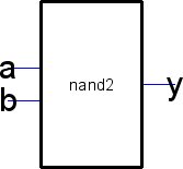 | Edit your "nand2{sch}" cell and use the Make Icon View command (in menu View). Electric will create a generic icon based on the exports as shown here. It will drop the icon in the schematic for handy reference; drag the icon away from the transistors so it leaves the schematic readable. |
| A schematic is easier to read when familiar icons are used instead of generic boxes. Modify the icon to look like this. Pay attention to the dimensions of the icon; the overall design will look more readable if icons are of consistent sizes. | 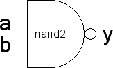 |
To edit the icon, click on it and use the Down Hierarchy command (in menu Cell / Down Hierarchy) or just type Ctrl-D. The Component tab will now show with various shapes (this is the "Artwork" technology). Delete the generic black box but leave the input and output wires. Turn on the grid.
The body of the NAND is formed from an open C-shaped polygon, a semicircle, and a small negating circle. To form the semicircle, create an unfilled circle node. Double-click to change its size to 6x6 and to span only 180 degrees of the circle. Use the rotate commands under the Edit menu to rotate the semicircle into place. Place another circle, adjust its size to 1x1, and move it into place. Alternatively, you can type "h" and use the arrow keys to move objects by 1/2 grid increments, then press "f" to return to full grid movement.
 | The Opened-Polygon node can be used to form the C-shaped body. When first created, it appears as a zigzag, shown here. To manipulate its shape, select it and enter "outline edit mode" by using the Toggle Outline Edit command (in menu Edit / Modes / Edit), or just type "y", or click on the icon in the toolbar. |
In this mode, you can use the left button to select and move points and the right button to create points. Since the default Opened-Polygon node has 4 points already, you should be able to form the "C" shape simply by clicking and dragging these points. Outline edit mode is not entirely intuitive at first, but you will master it with practice. When done, use the same command to exit the mode (just type "y"). See Section 6-10-1 for more on outline editing.
Electric is finicky about moving the lines with inputs or outputs. If you click and drag to select the line along with the input, everything moves as expected. If you try to move only the export name, it won’t move as you might expect. Therefore, make a habit of moving both the line and export simultaneously when editing icons. For appearance, remove the thin export connector lines. Replace these with bold black lines. You can easily do this by left clicking on a wire of the icon, then right-clicking, placing the cursor where you want the end point of the wire to be. Electric draws a wire that extends from the artwork of the icon.
| Use the "Text" item in the Component menu to place a label "nand2" in the icon. Make the text be 2 units high. | 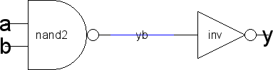 |
Now that you have an icon with three exports, create a new schematic called "and2" (don't forget to set the view to "schematic"). Use the Place Cell Instance command (in menu Edit) to instantiate a "nand2{ic}" and an "inv{ic}". Wire the two together and create exports on inputs "a" and "b" and output "y". Double-click on the wire between the two gates and give it a name like "yb" so you know what you are looking at in simulation. It is good practice to label every net in a design. When you are done, your "and2" schematic should look like this.
Next, create a new layout called "and2" (remember to select the "layout" view). Instantiate the "nand2{lay}" and "inv{lay}" layouts. ALWAYS use the Place Cell Instance command to create layout from pre-existing cells. NEVER build a cell by cutting and pasting entire existing cells. If you do, then make a correction to the original cell, your correction will not propagate to the new layout.
| Initially the cell instances appear as black boxes with ports. Select both instances and use the All the Way command (in menu Cell / Expand Cell Instances) to view the contents of each layout. Wire power and ground to each other. Move the cells together as closely as possible without violating design rules. You may need to place large blobs of pure layer nodes over the n-well and p-well to avoid introducing well-related errors from notches in the wells. Connect the output of the "nand2" to the input of the "inv" using Metal-1. Remember that connections may only occur between the ports of the two cells. Also connect the power and ground lines of the cells using Metal-2. Export the two inputs, the output, and power and ground. An easy way to do this is to use the Re-Export Everything command (in menu Exports) to bring exports to the surface level. | 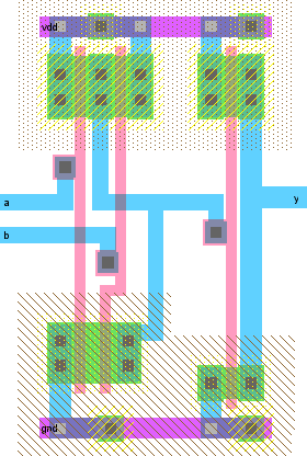 |
The Messages window shows how many ports were exported. The final gate should resemble this.
 |
Previous |  |
Table of Contents | Next |  |